


PFN is a conjugated polyelectrolyte used as an electron-interface in OPV devices to improve extraction efficiencies.Currently producing power conversion efficiencies of up to 7.1% at Ossila with further increases expected from additional optimisation and up to 9.2% reported in the literature [1-3].
Soluble in polar solvents such as water and methanol in the presence of small amounts of acetic acid.
General Information
| Full name | Poly [(9,9-bis(3'-(N,N-dimethylamino)propyl)-2,7-fluorene)-alt-2,7-(9,9–dioctylfluorene)] |
| Synonyms | PFN, PFN-DOF |
| Chemical formula | (C52H70N2)n |
| CAS number | 673474-74-3 |

Usage details
Inverted OPV devices were made using the architecture shown below with PFN (batch M221) as an electron-interface and PTB7:PC70BM in a 1:1.5 blend ratio (batches M211 and M113 respectively). Ossila's pixelated cathode substrate pack (S173) provided the device components.
Glass / ITO (100 nm) / PFN (5.5 to 10 nm) / PTB7:PC70BM (90 nm) / MoOx (15 nm) / Al (100 nm)
The substrate cleaning and PFN spin-coating were performed under ambient conditions with all other steps performed in an N2 glovebox until encapsulation had been completed (measurement performed under ambient conditions).
For generic details please see the fabrication guide and video. For specific details please see the condensed fabrication routine shown below. For information on our inexpensive Spin Coater for use with PFN please see our Spin Coater product page.
The active layer thickness, MoOx thickness, cathode metal (Ag or Al), PFN solution concentration, PFN drying/baking have not been fully optimised. As such, we expect further gains to be made with additional engineering work. However, for the devices made in this fabrication, a peak efficiency of 7.1% was achieved.

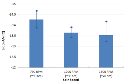
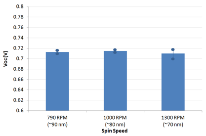
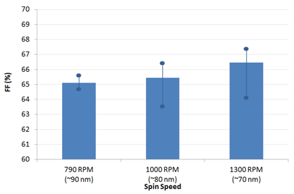

Note that some burn-in was observed (i.e. a small improvement in device performance after a few seconds under the solar simulator) and the variability of the devices is currently slightly higher than for other interlayers (average PCE of 6.7%). We expect the uniformity to improve with further improvements in PFN processing, in particular the optimisation of drying conditions to ensure that the acetic acid is fully removed prior to active layer deposition.